
Graphene molecular sensors (GMS) are an emerging technology that offer new possibilities in ion sensing, environmental monitoring, healthcare diagnostics and beyond. Known for its compact size, durability, high sensitivity and fast response times, the GMS has captured the interest of researchers and industry leaders alike. Its versatility even extends to disposable designs for single-use applications, such as biofluid analysis.
The core benefit of the GMS lies in its ability to detect subtle changes in electrical conductivity across a sheet of graphene. This sensitivity makes the GMS ideal for measuring minute variations in current, enabling the detection of specific molecules in gases, as well as tracking pH levels and identifying individual ions. Compared to traditional field-effect transistors, GMS’s adaptability allows it to function in environments and spaces inhospitable to conventional devices.
How GMS Delivers Precision in Sensing

GMS operate by exploiting the exceptional electronic properties of graphene. In Paragraf’s electrolyte-gated GMS, a sample droplet is placed on the sensing surface, creating an electrical bias between the gate electrode and the graphene channel. This bias shifts graphene’s doping level, visualized on an energy level diagram — a graph that maps the conduction and valence bands of the channel. Graphene’s energy level diagram’s symmetrical, hourglass shape pinpoints a “Dirac point”, where charge carriers encounter maximum resistance. As charge carriers move through this point, resistance peaks and decreases to reflect changes in conductivity. These variations form a transfer curve that reveals key characteristics, such as charge carrier mobility and resistance and enables precise detection of analytes.
Surface modifications can be used to further enhance the GMS’s selectivity. By functionalizing graphene with specific receptors or chemical groups, GMS can target specific analytes – from single ions to complex biomarkers.
Overcoming Challenges in Graphene Fabrication
Despite its promising attributes, previous attempts to functionalize graphene in these application spaces have failed to maintain consistent quality. Early attempts to create graphene electronics involved using chemical vapor deposition (CVD) to grow a layer of carbon atoms on copper foil. That layer would then be transferred onto an electronic substrate, introducing physical defects and contaminants that limit the graphene element’s effectiveness in high-sensitivity applications.
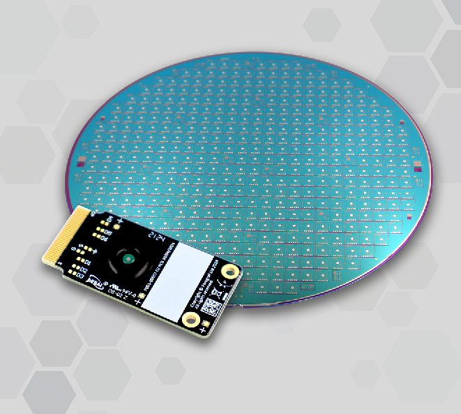
In contrast, Paragraf employs metal-organic chemical vapor deposition (MOCVD) to affect precise control over direct deposition of graphene onto substrates of common semiconductor materials such as sapphire and silicon, eliminating the need for transfer processes. This innovation substantially reduces defects and contamination, producing high-quality graphene suitable for advanced sensing applications.

A Flexible Platform for Research and Diagnostics
GMS are particularly appealing for their adaptability. After graphene deposition, sensor elements can be functionalized with custom receptors tailored to specific applications. These range from healthcare diagnostics using bioreceptors for disease markers, to environmental monitoring with ion-specific sensors.
Current manufacturing capabilities allow up to 32 GMS devices to be produced on a single 2-inch wafer, with plans to scale up to larger wafers and higher production volumes. This scalability positions GMS as a viable option for both research and large-scale diagnostic applications.

Multiplexing: Unlocking New Potential
One exciting capability of the GMS is its potential for multiplexing. By integrating multiple GMS on a single chip, researchers can simultaneously detect multiple analytes in a single sample. While current GMS chips typically contain 3-5 sensing channels, this capacity can be increased to as many as 100 channels per chip, based on application and customer demand.
Multiplexing is a game-changer for diagnostic applications, enabling the detection of numerous biomarkers or ions at once. Such innovations are paving the way for high-throughput screening in healthcare and complex environmental analyses. Detection methods can include microfluidic systems or applying liquid samples directly to the chip, offering flexibility across different applications.
Paving the Way for Future Applications

As GMS technology evolves, it is becoming a cornerstone for researchers and diagnostic developers exploring highly sensitive and robust sensing platforms. Its unique combination of precision, scalability and adaptability makes it a valuable tool for applications ranging from academic research to industrial diagnostics.
When Paragraf has compared its GMS to ones created with transfer graphene, they demonstrated superior robustness and sensing capability across multiple sensing channels and on a multiplexed diagnostic platform. This has been confirmed by third parties.
Find out more about how these versatile diagnostic platforms could be adopted in your sensing and monitoring programs by contacting our technical team today.
See for yourself
Check out some of our GMS Application Notes to find out some of the solutions our unique graphene is providing:
- pH Sensing with a GMS-PV01
- Potassium Sensing with a GMS-PV01
- Measuring Potassium Concentration in Serum
- Pyrene Deposition with a GMS-PV01
- Acetone Gas Sensing with a GMS-PV01
To experience the GMS’s molecular sensing capabilities for yourself, you can buy a quad pack directly from the Paragraf online store.