


Miracle Machine Man

In semiconductor manufacturing, the tools are almost as remarkable as the products they make. At Paragraf, some of the most specialised are built in-house.
If you ever meet Gavin Dodge, chances are you will begin to think of him as Q, the lead inventor in the James Bond series.
The comparison is not entirely unfair. Gavin is our Engineering Project Lead, and his job works something like this: a new project begins, requirements are drafted for testing the device, and then an idea for a machine or a tool that would enable it comes alive. Sometimes that tool simply does not exist yet, because nobody has needed it before. Gavin and his multi-disciplinary team design, build and test their creation, drawing on collaboration from right across Paragraf.
“Building your own tools is a major win as it enables us to provide early testing capabilities to enable data driven decision making for the company,” he says, with the understatement of someone who does this routinely.
Building for the leading edge
Paragraf works with a range of excellent equipment suppliers, and much of what happens in our foundry runs on industry-standard semiconductor tooling, that compatibility is central to how we make graphene manufacturable at scale.
But developing genuinely novel technology sometimes calls for genuinely novel tools. When you are working at the leading edge of material development, the requirement can be so specific to what you are doing that no established tool exists for it yet. That is where Gavin’s team comes in.
They design and build from off-the-shelf components where possible, or develop bespoke in-house mechatronics assemblies where the requirement demands it. Our software team writes the software to run them. The result is a tool shaped precisely around a Paragraf requirement, often one that did not exist as a requirement anywhere until we created it. Every tool is designed to current statutory regulation for UKCA certification.
Requirements evolve, too. New products to adapt tools for, changes in the size, colour or shape of devices. Gavin takes it all in his stride.
Probing, imaging and getting answers faster
Some of the most valuable machines Gavin and his team have built are probing and imaging tools that inspect wafers and determine whether they pass or fail. The team has developed a layer of machine learning to make that determination, and the results are automatically uploaded to Paragraf Systems for process engineers to view.
The significance of that is easy to miss if you have not done the job manually. Imaging and probing a batch of wafers used to take several days of hands-on work. Now the process is dramatically faster, requires far less manual intervention, and the results reach process engineers with minimal delay. The key is that the systems and data integration are designed in at an early stage of development, so the data flows straight to the people who need it.
That is not a marginal improvement. It changes how quickly the team can learn from what they are making, and in a business scaling a genuinely new manufacturing process, learning speed is everything.
Precision tools
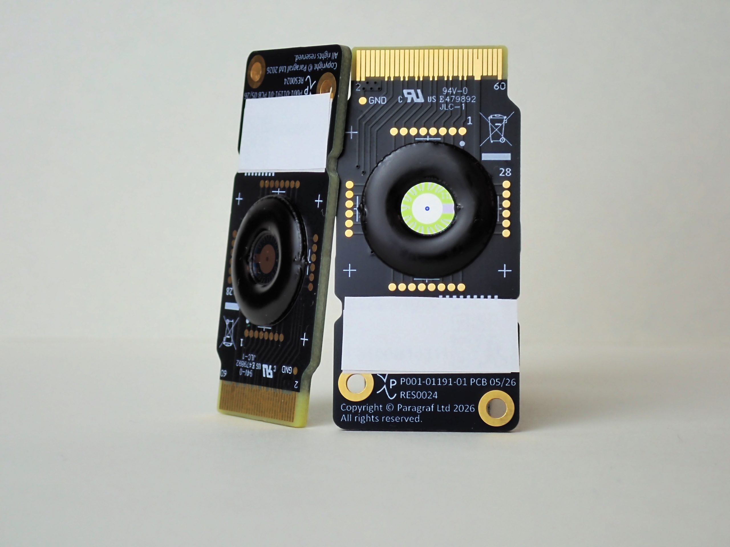
The latest piece of kit built by Gavin’s team handles the PMF2000, Paragraf’s three-channel GFET. A robot picks the device PCB from standard trays and places it into a testing slot; the devices are imaged, and a fluid dispensing system then delivers a precisely controlled volume onto the device to check its characteristics. Robotic assemblies move the devices safely throughout.
Gavin demonstrated the manual process alongside the automated one. The difference was immediately visible. A person doing this by hand is skilled, careful and consistent, but within human limits. An automated system dispensing a controlled volume, with robotic handling and automated testing, holds tolerances a person simply cannot.
“Fitting this motor on”
Ask Gavin about one of the team’s biggest wins and the answer is characteristically undramatic: fitting a motor.
What that motor does is worth explaining. Adapted to fit, it allows the camera system to automatically adjust a turret to move between optical lenses, from 2.5x magnification all the way to 50x. At the low end, you see the whole device. Then the whole square. At 50x, the entire graphene area is viewable.
One motor, adapted by hand, turning a fixed instrument into something that moves fluidly from the big picture down to the fine detail, and back again. That range is what lets engineers understand what is actually happening on a wafer.
Developing as we go
Perhaps the most valuable thing about having someone like Gavin in the building is not any individual tool. It is the ability to adapt.
“Supporting a developing company that requires rapid solutions to enable the development of graphene devices is what the business needs,” is how he describes it. “We call on the team’s experiences from a wide range of industries to enable us to rapidly develop solutions. These projects enable the internal training of future apprentices.”
The requirements are not handed down from a catalogue. They emerge from the work itself: an engineer hits a limitation, describes the problem, and a solution gets built. Then the next limitation. Then the next.
That is what it looks like to build a manufacturing capability that has never existed before. The products are new, the processes are new, so it follows that some of the tools have to be new as well.
What excites Gavin most about his job? Enabling talented people to develop incredible technology.
Paragraf is the world’s first graphene electronics foundry, manufacturing graphene-based electronic devices at scale in Huntingdon, Cambridgeshire. Find out more at paragraf.com