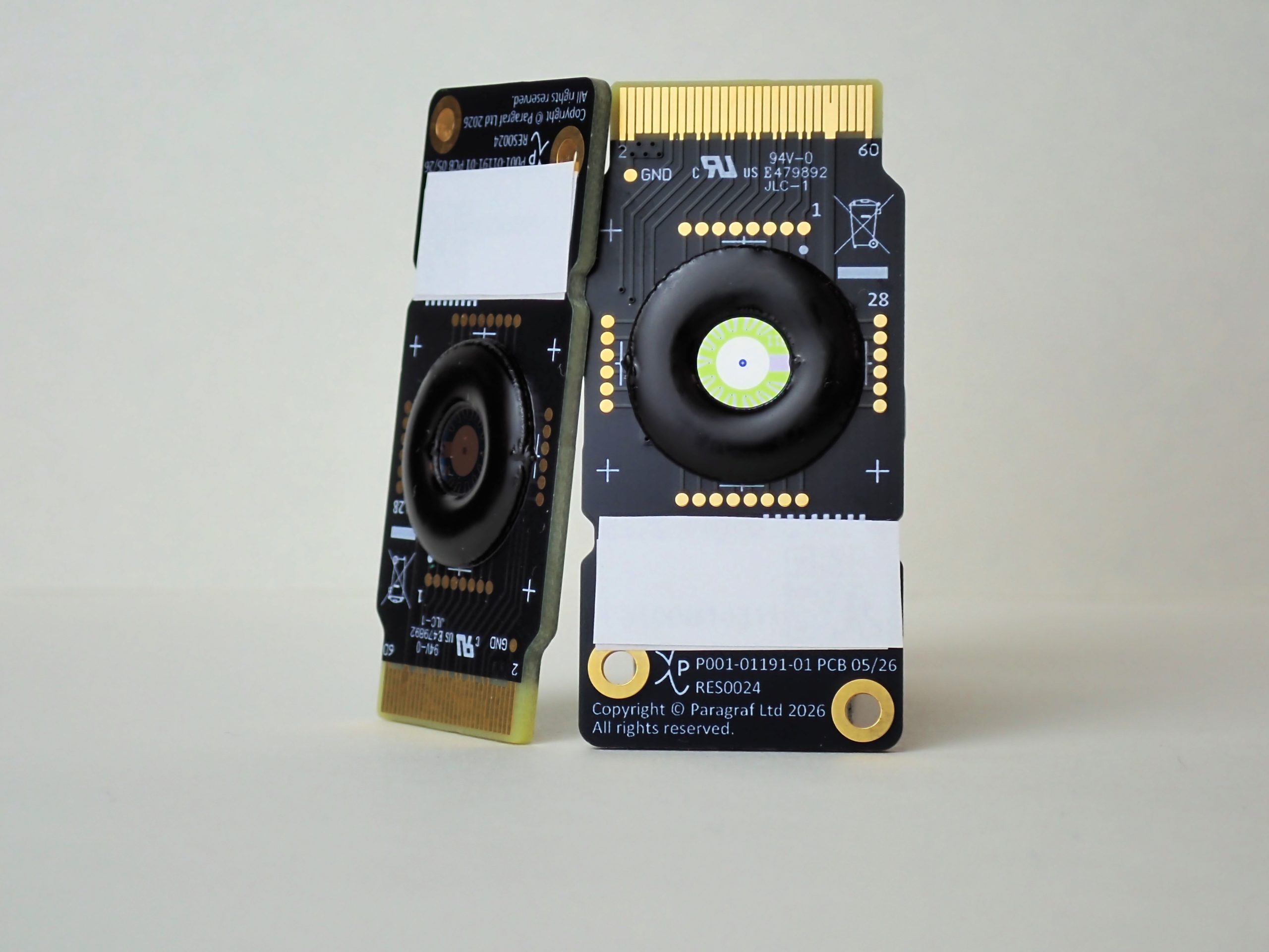




Huntingdon, UK , 29 September 2026 – Paragraf, the world’s first foundry for 2D electronics, today announces an expansion to its 2D materials production capabilities, producing molybdenum disulphide (MoS₂), an ultrathin 2D semiconductor, in addition to the firm’s graphene capabilities. This extremely thin material offers dramatically lower power usage in next generation electronic devices.
Paragraf is a lead industrial partner for a £6.4 million EPSRC-funded research programme developing molybdenum disulphide (MoS₂) electronics, aimed at dramatically reducing the energy demands of data centres and high-performance computing. The programme is titled “Enabling Net Zero and the AI Revolution with Ultra-Low Energy 2D Materials and Devices (NEED2D).”
The programme brings together Queen Mary University of London (QMUL) with 22 industrial partners spanning the full supply chain, from precursor chemicals and growth equipment through to device end users. Paragraf is currently the sole supplier of 2D materials.
Tackling the problem at its source
The growth of artificial intelligence has driven an unprecedented rise in data centre energy consumption. The prevailing response has been to build more generating capacity, at a cost of billions of pounds. This programme takes a different approach: reducing demand at source by addressing why computing consumes so much energy in the first place.
Data centres consume electricity on this scale because the devices inside them are inefficient. Every computer contains silicon transistors, and a significant proportion of the energy they draw is lost as heat rather than spent on computation. Silicon was initially an excellent choice. However, as devices have scaled to smaller geometries, driven by processing speed, the current leakage and power inefficiencies of these device architectures has spiralled.
MoS₂ offers a route to substantially more efficient devices. It is a semiconductor, the class of material at the heart of every transistor, but structurally it resembles a three-atom sandwich, with a layer of molybdenum between two layers of sulphur. Transistors made with a channel of monolayer MoS2 exhibit a high on/off current ratio with an extremely low leakage current when in the off state, due to their thinness, making them highly power efficient. MoS₂ can be integrated onto existing silicon structures or operate as a standalone semiconductor, offering the potential to scale, beyond the fundamental limits of silicon. The programme is targeting devices that consume up to 90% less energy than conventional silicon equivalents.
Paragraf’s role
Paragraf will supply high-quality, large-area MoS₂ to the research programme, drawing directly on the process expertise developed producing the world’s leading wafer-scale graphene. The company is the principal industrial partner in the programme and will work in close collaboration with Queen Mary University of London on device research.
Dr Simon Thomas, CEO and Co-Founder of Paragraf, said: “Paragraf has spent years learning how to grow high-quality two-dimensional materials at scale, and MoS₂ is a natural extension of that capability. This programme is a clear example of the world-leading research which the UK excels at, with a clear industrial route, a complete domestic supply chain, and sovereign capability in the materials that will underpin the next generation of computing. This is exactly the type of research that will make the UK’s AI superpower ambitions a reality.”
Professor Sir Colin Humphreys CBE FREng FRS, of Queen Mary University of London, and the Project lead in the RPSRC-funded project, said: “We lived through the silicon age, and we are now working to succeed it. Silicon transistors lose more energy to heat than they spend on calculation, and that inefficiency is now being multiplied across every data centre in the world.”
“2D materials such as MoS₂ offer an exciting route towards more energy-efficient electronics. Paragraf has already demonstrated wafer-scale production of high-quality MoS₂, building on its pioneering expertise in large-area graphene. This collaboration marks the next step in developing and applying that capability to electronic devices, with the potential to deliver a new generation of more energy-efficient technologies.”
A complete UK supply chain
The programme has been structured to include every stage required to take the technology from material to device, including precursor chemicals, growth equipment and end users. Partners span UK chemical suppliers, equipment manufacturers and technology companies, giving the research a direct route to industrial application.
About Paragraf
Paragraf is the world’s first foundry for graphene and 2D material electronic devices: designed, developed and manufactured at scale in the UK. With a proprietary process to grow high purity 2D materials directly on standard semiconductor industry substrates, Paragraf has pioneered the delivery of two-dimensional technologies at scale. Paragraf has unlocked the incorporation of these remarkable materials into both existing and new electronic devices and applications.
Through our world-first dedicated graphene device foundry in Huntingdon, Cambridgeshire, Paragraf delivers high-performance, low-power technologies to multiple markets and offers two-dimensional-material foundry services to customers and partners. Established in 2018 and backed by more than $150 million in private investment, Paragraf operates across five sites on three continents, with teams in the United Kingdom, the United States, China and the United Arab Emirates, serving customers worldwide.
For more information, technical specifications, or to discuss evaluation opportunities, contact sales@paragraf.com
If you are a research or academic institution and are interested in our 2D devices, please contact enquiries@paragraf.com
— END —
Contact
Paragraf
Shivani Lodhia, Corporate Communications
or
Parisi Consulting
Notes to Editors
About NEED2D
Enabling Net Zero and the AI Revolution with Ultra-Low Energy 2D Materials and Devices (NEED2D) is a £6.4 million research programme funded by the Engineering and Physical Sciences Research Council (EPSRC). The programme brings Queen Mary University of London together with 22 industrial partners representing the full technology supply chain. The research focuses on the development of electronic devices based on two-dimensional materials, including molybdenum disulphide (MoS₂), with the aim of developing technologies that could substantially reduce energy consumption compared with conventional silicon electronics.
For more information, please visit: https://www.need2d.com/
About molybdenum disulphide (MoS₂)
Molybdenum disulphide is a two-dimensional material consisting of a layer of molybdenum atoms between two layers of sulphur atoms. Its electronic properties make it a promising material for future generations of ultra-low-energy electronic devices.