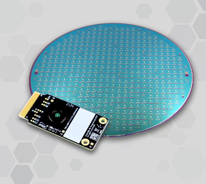


 Paragraf, the UK-based company pioneering the commercialization of graphene-based electronics using standard semiconductor processes, has successfully produced the first 6-inch wafer at its new manufacturing facility in Huntingdon, marking a significant expansion in the company’s production capability and technology platform.
The wafer contains graphene field-effect transistors (GFETs) fabricated using Paragraf’s proprietary process in which graphene is grown directly on silicon. This achievement represents a major step forward for scalable graphene electronics and is believed to be the first demonstration of GFETs on silicon using a direct-growth approach at this wafer size.
Until now, Paragraf has produced GFETs on 2-inch sapphire wafers using its contamination-free, transfer-free graphene growth technology. While other approaches to GFETs on silicon typically rely on transferring graphene from a growth substrate, often introducing metallic contamination, Paragraf’s direct-on-silicon process preserves material purity and device integrity while opening the door to greater compatibility with mainstream semiconductor manufacturing.
The transition from 2-inch to 6-inch wafers is a major milestone, enabling higher throughput, improved uniformity, and closer alignment with established semiconductor fabrication infrastructure. Together with the development to include silicon substrates, this positions Paragraf to accelerate the development of scalable graphene-based electronic and sensing devices.
“This first 6-inch wafer out of our Huntingdon facility is a landmark moment for Paragraf,” said Simon Thomas, Co-Founder and CEO of Paragraf. “It demonstrates both the maturity of our graphene growth technology and our ability to scale it on industry-relevant substrates, while maintaining the contamination-free advantages of our approach required by many applications and customers.”
The new Huntingdon facility is a cornerstone of Paragraf’s long-term manufacturing strategy, supporting the transition of graphene electronics from laboratory-scale innovation to commercial-scale production.
About Paragraf
Paragraf is the world’s leading graphene-based electronic device design, development and manufacturing company. Building on our proprietary process to grow graphene directly on standard semiconductor industry substrates, Paragraf has pioneered the delivery of two-dimensional technologies at scale. Paragraf’s high-quality graphene – integratable with standard semiconductor tool process lines – has unlocked the incorporation of this remarkable material into both existing and new electronic devices and applications. Through our world-first dedicated graphene device foundry, Paragraf delivers high-performance, low-power technologies to multiple markets and offers two-dimensional-material foundry services to customers and partners, providing graphene in chips to their device requirements.
— END —
Contact
Paragraf
Matt Enderle, Corporate Communications
media@paragraf.com
or
Parisi Consulting
paragraf@helloparisi.com