

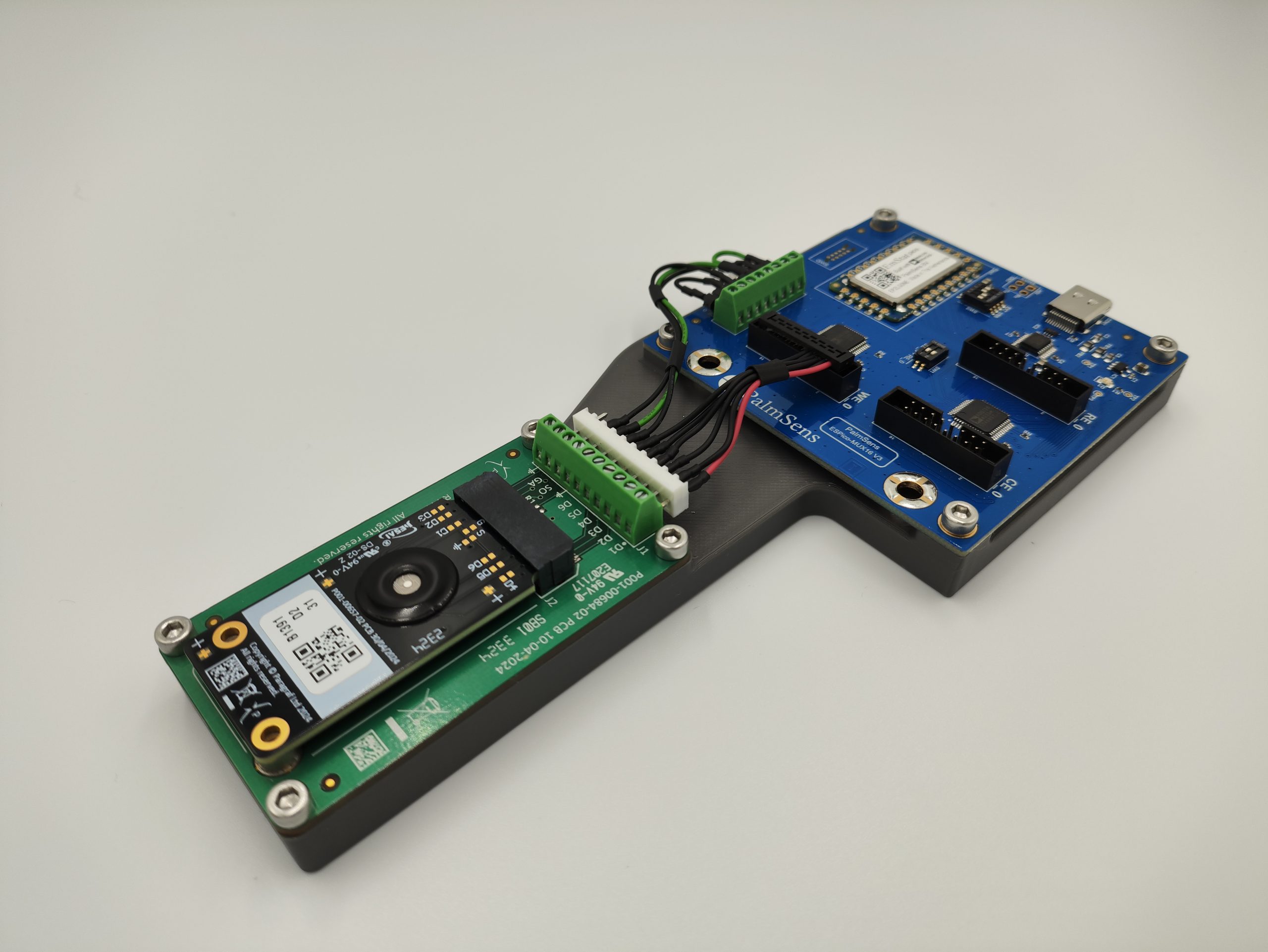
Paragraf is ushering in a new generation of solid-state devices and VLSI circuits, enabled by 2D materials.
Our unique, silicon-compatible, wafer-scale processes are scalable and eliminate major hurdles to commercialisation, such as material purity and cost. And behind our device designs and manufacturing processes are an expert team of material scientists and device physicists, who are constantly innovating.
Applications
Learn about how our technologies can be applied to your products
FEATURE AND BENEFITS
Why Paragraf
Paragraf is a collaborator, that is building a world-leading position in the design and manufacture of devices and chips, enabled by graphene and other 2D materials.
- Silicon compatible processes
- Deploys on to a range of substrates
- Range of 2D materials possible
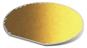
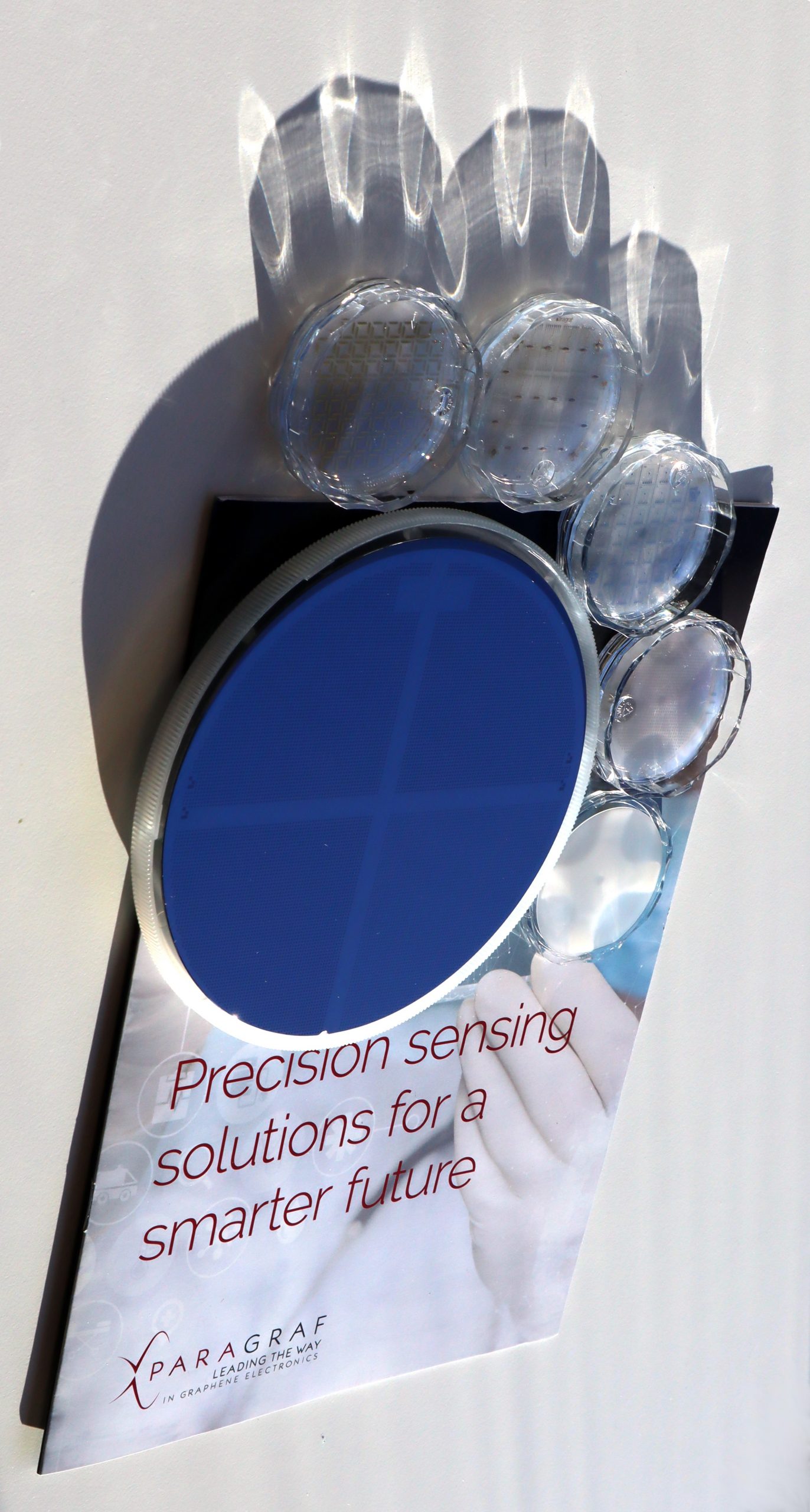
- Wafer-scale technology
- Scalable solution
- Integrates with existing manufacturing infrastructure
Articles


At Paragraf we are always interested in working with our customers and research partners to understand how our high-purity 2D graphene devices can be used in new applications.
FEATURE AND BENEFITS
Have an interesting idea?
If you have ideas about new applications for our Solid State Technology, we would love to hear from you.
Articles