
By Simon Thomas, CEO at Paragraf
Ever since graphene was first mechanically exfoliated back in 2004, it has ignited renewed fervour within the materials science domain – thanks to the incredible things that can prospectively be done with it. The following article will focus on how, in the years ahead, it could revolutionise semiconductor engineering.
Graphene monolayers are made of single atom thick deposits of carbon. Because of the nuclear bonds holding these atoms together, the resultant structure has exceptional strength. The robustness of this material means that it is able to function within the most challenging of operational environments (handling heightened temperatures and large breakdown voltages). Alongside this, graphene offers elevated levels of electron mobility (over 130x greater than silicon), which translates into extremely attractive conductivity characteristics.
Graphene’s Value in Different Branches of Electronic Engineering
There are several key areas within microelectronics that could benefit from the use of graphene. Among these are:
- Power Systems – Complementing wide bandgap semiconductor technologies (namely silicon-carbide and gallium-nitride), graphene would be able to augment their operation. This would lead to faster switching speeds and markedly heightened efficiencies.
- Optoelectronics – Graphene’s high optical transparency means it could be employed in displays (providing an alternative to the indium tin oxide films that are currently used).
- Data Processing – The addition of graphene to high density microprocessor resources could substantially accelerate throughput figures. This would allow an extension to the longstanding ‘Moore’s Law’, that has defined the semiconductor industry for many decades, by overcoming the power leakage problems that arise with the move to ever smaller process nodes.
There is considerable potential in an array of other market segments too – including energy storage, solar power, body-worn medical equipment, the Internet of Things (IoT) and sensors.
Sensors present some very lucrative opportunities for graphene. Analyst firm Research & Markets estimates that the worldwide graphene-based sensors business will be worth around $980 million annually by 2024. Among the key uses outlined in its recent report are biosensors and optoelectronic devices. In respect to electrical sensors particularly, it is felt graphene has the attributes needed to make a difference in the near future. However, the success of this material in such areas is very much dependent on having an effective method of production.
Through access to exfoliated graphene flakes, it has been possible to produce certain microelectronic devices in small quantities. However, by its very nature, the global microelectronics industry simply doesn’t work like that. It’s all about large volumes of devices being manufactured at low unit costs, thanks to economies of scale. If graphene is to be successfully incorporated into a new breed of microelectronic devices, then the procedure used for its synthesis must be fully aligned with semiconductor fabrication processes.
Synthesising Graphene to Meet High Volume Requirements
The main methods used for large area graphene synthesis currently rely on chemical vapour deposition (CVD) and plasma-enhanced chemical vapour deposition (PECVD). It must be noted that both of these processes have significant issues associated with them.
Graphene production using CVD/PECVD methodologies sees synthesis take place on a metal catalyst (usually either a copper or nickel foil), as opposed to the actual semiconductor substrate. The synthesised graphene must then be removed from the metallic foil and transposed onto the semiconductor substrate. As a consequence, ensuring both the purity and the structural integrity of the graphene produced via these methods is extremely difficult. The presence of contaminants poses a real threat. This could be in the form of chemicals employed in the transfer process or traces of metal foil remaining after the catalyst has been etching away. These contaminants or structural anomalies can have a detrimental effect on the synthesised graphene’s performance parameters.
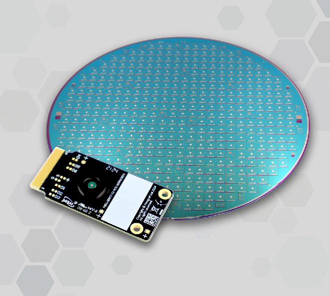
The metalorganic chemical vapour deposition (MOCVD) process that has been developed by Paragraf means that CVD and PECVD are no longer the way forward for graphene synthesis. This proprietary process is truly unique, as it enables the large scale production of graphene – along with other two-dimensional (2D) materials. Unlike the CVD/PECVD arrangements already discussed, that call for transfer from the original catalyst, MOCVD allows the graphene material to be layered directly onto the semiconductor substrate. The inconvenient transfer step can be circumvented and contamination is thus no longer deemed a problem.
Graphene can be placed directly onto full-size semiconductor wafers in a consistent and completely reproducible manner. This means that IDMs and foundries will be able to incorporate the MOCVD process into the workflows that they have already established, without any disruption being experienced.
Graphene-Based Magnetic Sensor Devices
One of the early openings for graphene is within the Hall-Effect sensor market. Deployed into a wide range of industrial and automotive systems, these sensors provide a non-contact mechanism via which the flux density of magnetic fields can be determined.
Conventional Hall-Effect devices have a three-dimensional (3D) sensing element, where the depth of this element can unduly influence the results obtained. Magnetic field components that are not perpendicular to the sensing element’s orientation may contribute to the detected field strength, thereby giving a false figure. This phenomenon is referred to as the ‘planar Hall-Effect’.
Differentiating between the real signals and the false ones means that extra components need to be included in the signal conditioning circuitry (thus increasing the bill-of-materials costs). Otherwise mathematical modelling, might be called for – though this will not be applicable in situations where real-time measurement data is required (such as vehicle safety systems, etc.). Other downsides associated with conventional Hall-Effect sensors include a fairly limited dynamic range and accuracy being affected by temperature variations.
Since graphene is a 2D material, it has a major advantage when it comes to the accurate measurement of magnetic fields – since the thickness of the sensing element will not need to be factored in. Hall-Effect sensors that utilise a graphene monolayer rather than a conventional sensor element will be able to support higher degrees of accuracy, as any errors caused by the planar Hall-Effect can be eliminated. Other plus points to consider include the greater thermal stability that graphene exhibits – which means that any device using this for its sensing element will not be as exposed to inaccuracies caused by temperature fluctuations. This will allow such devices to be deployed in applications where there are extreme temperatures to contend with.
Admittedly, graphene-based Hall-Effect sensors have been seen before, but these could only be produced in small batches that had large unit costs – with no way of achieving the necessary economies of scale previously discussed. Thanks to the MOCVD process, Paragraph’s GHS series sensors can be produced in the volumes expected by industrial and automotive customers. These devices are not subject to the planar Hall-Effect, as they rely on a graphene monolayer. As a result, they offer greater exactitude when it comes to determining the strength of magnetic fields. They deliver nT resolution levels without the need for additional signal conditioning hardware. Consequently, the sensor system is more streamlined. In addition, they have a greater dynamic range than conventional Hall-Effect sensors, along with improved temperature stability and superior linearity.
By leveraging a game-changing synthesis process, it has finally been made possible to apply graphene (and the numerous operational advantages that come with it) to commercially produced microelectronic devices. Electronic component manufacturers now have access to large-area graphene through Paragraf, without being hampered by contamination issues. Though there were numerous attempts in the past to make graphene viable within a microelectronics context, this is the first time it has really been accomplished in a way that adheres to the high volume production requirements that this industry sector mandates.