
Paragraf Introduces PMF2000 GFET
HUNTINGDON, England [12 May 2026] – Paragraf, the Cambridgeshire-based global leader in the commercialisation of graphene-based electronics, is expanding its Graphene Field Effect Transistor (GFET) product line with the introduction of PMF2000 GFET.
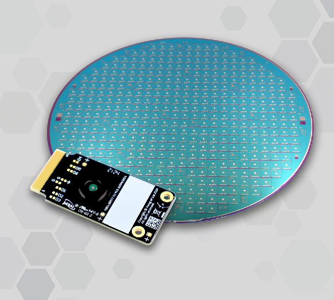
The company is continuing growth of its product portfolio with the release of the PMF2000 GFET, another pristine, contamination-free layer graphene device. This is the first device to come from the company’s new, large-wafer manufacturing facility – the world’s first graphene foundry – in Huntingdon. This production progress increases the overall yield of devices and sets a new benchmark for consistency of quality, allowing Paragraf’s customers to meet their molecular sensing needs at industrial scale.
![]()
The foundry enables Paragraf to produce a sensor that will give customers reliable and repeatable results at high volume without changing the design or function of the chip, while offering the flexibility of fully customisable designs purpose configured for the application. Customers who have employed the original version of the GFET will enjoy a seamless transition to the PMF2000, with the option to order the sensors in much higher volumes.
‘The PMF2000 GFET’s graphene-on-silicon construction represents the strongest demonstration yet that Paragraf’s proprietary graphene technology has unlocked the future of increased performance semiconductor production,’ said Dr. Simon Thomas, Co-Founder and CEO of Paragraf. ‘We look forward to seeing our customers use this device to break new ground in healthcare, agritech, chemical and industrial applications.’
PMF2000 GFET devices are available now at Paragraf’s online store at https://store.paragraf.com/ where customers who are interested in learning more about what the device can do may access a series of application notes that provide experimental operations they can perform in their own labs.
About Paragraf
Paragraf is the world’s leading graphene-based electronic device design, development and manufacturing company. Building on our proprietary process to grow graphene directly on standard semiconductor industry substrates, Paragraf has pioneered the delivery of two-dimensional technologies at scale. Paragraf’s high-quality graphene – integratable with standard semiconductor tool process lines – has unlocked the incorporation of this remarkable material into both existing and new electronic devices and applications. Through our world-first dedicated graphene device foundry, Paragraf delivers high-performance, low-power technologies to multiple markets and offers two-dimensional-material foundry services to customers and partners, providing graphene in chips to their device requirements.
— END —
Contact
Paragraf
Matt Enderle, Corporate Communications
media@paragraf.com
or
Parisi Consulting
paragraf@helloparisi.com