
By Simon Thomas, CEO, Paragraf
Over the last decade or so, graphene has gained an ever-increasing amount of press attention, due to the incredible properties it possesses and its potential to enhance all manner of different products. Comprising a monolayer carbon lattice with strong atomic bonds, graphene’s key attributes include high levels of mechanical stability (having tensile strength 200x that of steel), outstanding electrical conductivity (an order of magnitude higher than copper) plus extraordinary thermal conductivity (currently the highest of any known material). The much talked about prospect of it boosting performance in electronic devices is, however, yet to be leveraged effectively. The reason for this stems from the way in which this material is manufactured and processed. An innovative new approach to graphene fabrication is now set to change things, with the first place where it will see significant commercial traction being magnetic sensors.
A long established stalwart of electro nic system design, the Hall-Effect sensor serves a pivotal role in a wide variety of different application spaces. These sensors are used to determine the magnetic fields present within their surrounding environment, and through this the positioning or movement of mechanical apparatus (such as the steering column of an automobile or the rotor in an industrial motor drive system). Elsewhere these units are employed to monitor the currents passing through electrical infrastructure (generated by photovoltaic panels, for instance).
This is a major league business – the already sizeable global magnetic sensor market (of which Hall-Effect sensors represent the majority) is steadily growing, predicted to be worth $3.5 billion by 2025 (according to research compiled by analyst firm Global Market Insights). Despite their widespread usage, there is still scope to increase Hall-Effect sensor application usage, particularly with higher performance devices, and this is a clear opportunity for graphene to show its value.
Conventional Hall-Effect Sensor Shortcomings
Something that has always proved problematic with conventional Hall-Effect sensors is that the sensing element is three-dimensional (3D). Its depth leads to false measurement signals being produced that emanate from the in-plane magnetic field component, rather than the perpendicular one; referred to as the ‘planar Hall Effect’. Such false signals interfere with the real signals and give the impression that there are additional magnetic poles present – which is of course not actually the case. Referred to as ‘pseudo-multipoles’, these will mean that measurement accuracy is impacted upon. Though the real signals and the false signals can be separated from one another using additional circuitry, this will add significantly to system complexity and power consumption, limit the operational temperature range and push up cost. Other downsides associated with conventional Hall-Effect sensors include a fairly limited dynamic field range and measurement bandwidth, plus a low measurement resolution (which is fundamentally limited by thermal drift and a high thermal noise floor).
As graphene is a two-dimensional (2D) material, consisting of just an atom-thick monolayer of carbon, it is not susceptible to the in-plane field component and it displays a very low thermal noise floor. Hence using it in magnetic field measurement enables significantly more accurate results to be derived. It is also worth noting that the thermal stability of graphene mitigates thermal drift. Let’s next look at the reasons why.
Difficulties Concerning Graphene Production
It has to be acknowledged that the current most common methods for fabricating graphene are not very well aligned with high-volume commercial-grade electronics production requirements. There are basically two main options. The first method is exfoliating graphite. This can deliver good quality graphene, but it is typically over a very small area, cannot be customised to fit with specific end use requirements and can be multi-layered and non-homogeneous. These attributes seriously limit its effectiveness in a microelectronics context.
The other method is to synthesise graphene on some form of metal substrate, most commonly a copper foil. Graphene fabricated in this way needs to be transferred onto an electronics compatible substrate afterwards. There are several different transfer processes that can be employed for that purpose – though none is ideal. They can potentially impinge on how the graphene functions in an electronic device, by either contaminating the graphene or damaging its structure.
For many of the transfer processes it is simply not possible to remove all of the copper atoms. The chemicals used in wet transfer processes can also remain present too. These metallic impurities and chemical contaminants have a detrimental effect on the graphene properties and hence any subsequent device performance. Conversely ‘dry’ transfer methods can result in defects within the graphene itself – the quality of the graphene is thus not of the expected standard and the full benefits of its properties cannot be realised.
A New Approach to Fabricating Graphene
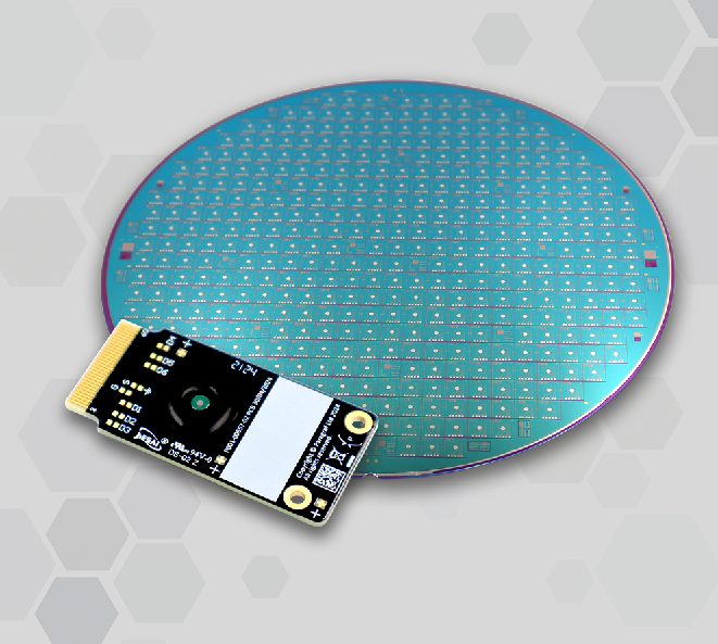
The objective of Cambridge University spin-out Paragraf is to revolutionise the electronics industry by harnessing the unique characteristics of graphene. Through the novel, scalable process that its engineering team has developed, it is possible to produce single-atom thick layers directly onto widely-used crystalline semiconductor wafer substrates – such as silicon (Si), silicon-carbide (SIC), sapphire and gallium-nitride (GaN). Consequently, the contamination issues that transfer activities cause can be circumvented, with the upshot that commercially viable devices incorporating graphene may be produced in volume.
The graphene produced by this method can cover a wide area (addressing full size 8-inch wafers), with much better uniformity. Also reproducibility is assured, so there will be minimal variation in end product quality, and the process is compatible with existing electronic device manufacturing procedures and equipment. Furthermore, while other graphene production/transfer processes mean there is little flexibility, the ground-breaking Paragraf process permits the electrical and mechanical properties of the manufactured graphene to be tuned at the point of production. Inclusion of expensive post-processing techniques can thus be avoided.
Graphene Hall-Effect Sensors
The Hall-Effect sensors produced using this proprietary process have set new performance benchmarks. As the active sensing element in each device is comprised of a single atom-thick graphene monolayer, the influence of the planar Hall Effect has been totally eliminated. These devices deliver 30x greater sensitivity than the conventional silicon-based options and have better operational stability. Their clear benefits will make them appealing to scientific research, healthcare, avionics, automotive, satellite production, robotics and numerous other industry sectors. 
Figure 1: Paragraf’s GHS Series Hall-Effect Sensors
Paragraf sensors can support resolution figures that are down at nT without the need for flux concentrators or the addition signal conditioning ICs (to amplify or filter the signal). This means the system complexity can be reduced and the overall bill-of-materials cost is kept in check. These devices can be used in a broad range of magnetic fields – reaching all the way up to ±9T. Their elevated mobility translates into faster responsiveness and a wider dynamic range. They also have far better linearity (with less than 0.5% deviation normally). Capable of operating down to 10nA, they have a substantially lower power budget than conventional sensor devices. Another key advantage of graphene-based Hall-Effect sensors is the wide temperature range they can support. The sensors can be used in cryogenic application settings of -271°C all the way up to the 80°C temperatures expected in automotive and industrial use cases. Moreover, higher temperature variants are currently under development which will further extend the possibilities that these devices can address.
Thanks to the mechanical strength of graphene, these new Hall-Effect sensors exhibit exceptional robustness, which means that a prolonged operational lifespan is assured. Resilience to electro-static discharge (ESD) enables them to be used in the most uncompromising of environments. The low power dissipation of these sensors (which is in the order of pW) means they will not heat cryogenic environments.
Conclusion
As we have seen, there are certain shortfalls that are inherent to standard Hall-Effect sensor devices – in terms of their sensitivity, accuracy and the effect that temperature can have on their operation. The new graphene-based GHS series sensors developed by Paragraf will be able to support operational parameters that go way beyond what conventional devices can achieve. As graphene is a 2D material (with a single atom thickness) it does not have the planar Hall-Effect issues that would normally be witnessed, with only the perpendicular magnetic field being registered by the sensor element. Accuracy figures are thereby improved, with no false signals induced. Graphene-based Hall-Effect sensors therefore provide an energy-saving solution that proves far better at determining magnetic field values, while still allowing for the economies of scale that volume production enables.