
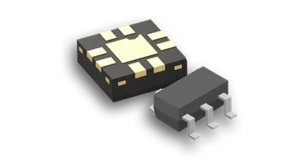
Paragraf Graphene FET
GFET-PV01
Available Now
Our Products
Graphene Hall Sensors (GHS)
High-performance graphene-based magnetic sensors for current sensing and position sensing delivering higher sensitivity and superior noise tolerance.
Graphene Field-Effect Transistors (GFET)
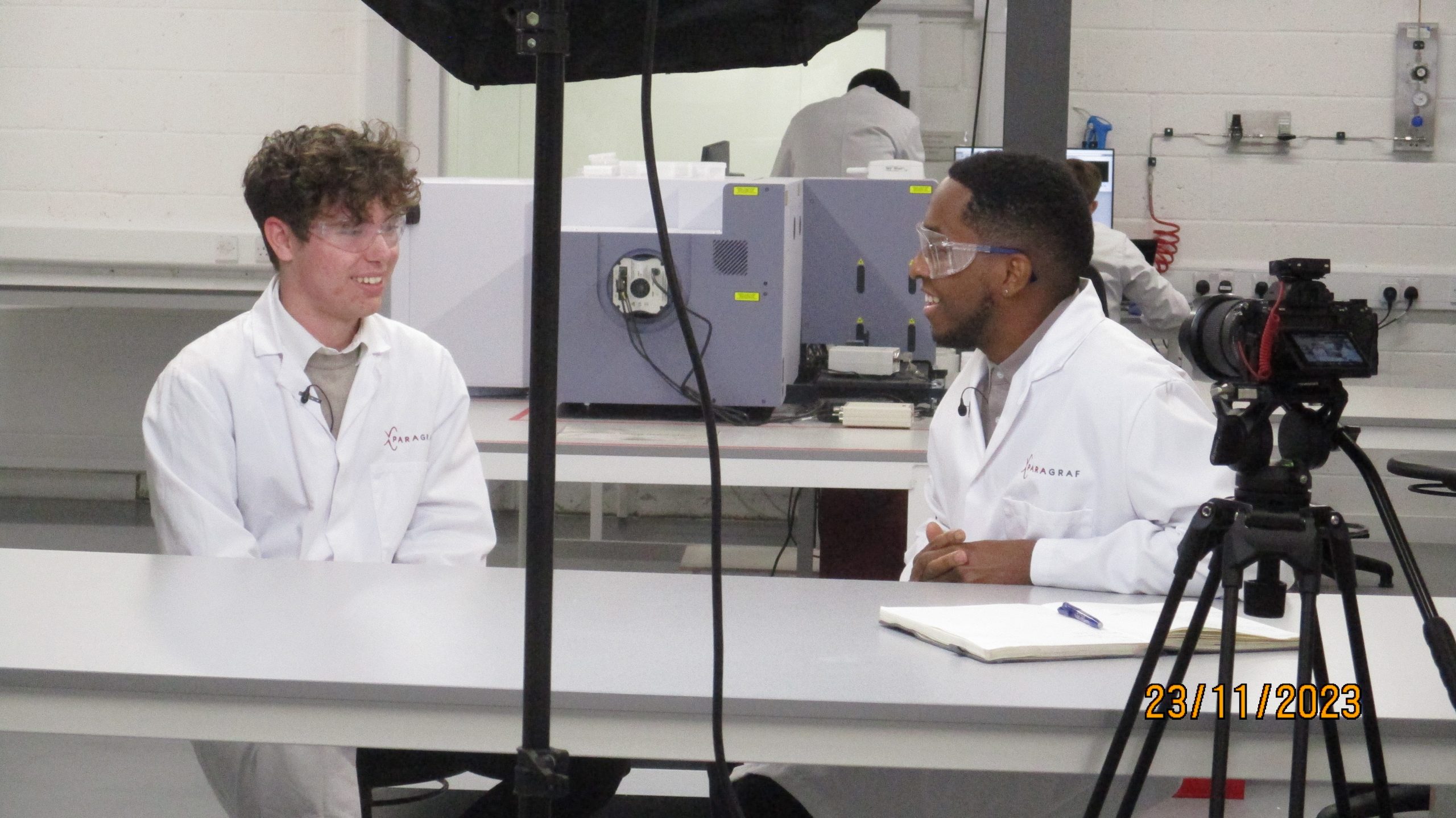
Paragraf GFET-PV01: Mass-produced electrolyte-gated FET with direct graphene deposition, homogeneous electric field during operation and versatile sensing applications.
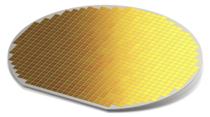
Custom Foundry Services
Paragraf is ushering in a new generation of solid-state devices and VLSI circuits, enabled by 2D materials with custom deposition and foundry services.
Industries

Automotive
Make your EV safer by preventing thermal propagation and reducing the risk of injuries and fatalities from road traffic collisions.

Agri-tech
Deliver precision agriculture with graphene sensors monitoring air, soil, crop and animal health. Transform the sustainability and security of our food system.

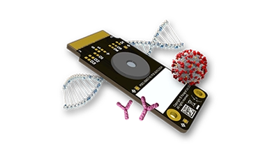
Healthcare
Achieve more accurate and rapid biomarker discovery, detection and characterisation to accelerate disease research and improve health.

Automation
Optimize process control, enhance quality control, and improve production and energy efficiency of your automation system.

New updates
Read what we have been up to with our latest news and articles


Our vision

Healthy People
Graphene biosensors will deliver faster time to results, and reduced sample preparation times. Precision farming will also be revolutionised leading to healthier foods and environment.

Healthy Cities
Cities around the world will achieve their clean-air goals enabled by Electric Vehicles. Manufacturers will be able to provide safer and more efficient use of batteries and more efficient motors.

Healthy Planet
2D material based transistors have the potential to dramatically improve the performance density and reduce the energy footprint of the compute infrastructure worldwide.