By John Tingay, CTO, Paragraf.
Comprised of a single layer of carbon atoms, with an incredibly strong structure, graphene has been much heralded in the field of materials science. The properties that it possesses have considerable appeal across a broad spectrum of industry sectors. For several years, it was perhaps difficult to see through the hype and speculation surrounding this material, now there are well-defined places identified where it is certain to make a real difference. Because of the exceptional attributes it possesses, there is currently a lot of interest in its use within next generation microelectronics.
Graphene exhibits very high electron mobility, and this translates into unmatched conductivity. Thanks to its high optical transparency, there are a multitude of opportunities that could be explored within optoelectronics – such as in displays (where it could offer an alternative to indium tin oxide films). The properties of graphene also lead to benefits across a wide range of sensors, mechanical, electronic and biological.
It also has value from a power electronics perspective. Here it could be used in tandem with emerging wide bandgap semiconductor technologies – namely silicon-carbide (SiC) and gallium-nitride (GaN). Since it can comfortably cope with the elevated breakdown voltages and temperatures that SiC/GaN devices support, it is uniquely positioned to augment their operation.
Through the implementation of graphene in computing logic, there is the prospect that processing rates could be dramatically increased, thereby revolutionising high performance computing (HPC). Photovoltaic cells and batteries could be boosted too. In addition, the power budgets associated with graphene-based devices will be significantly lower. This is something that could undoubtedly be exploited by IoT networks, wearable healthcare monitoring, electric vehicles, and suchlike. Finally, since graphene-based devices will be capable of operating at much lower temperatures, there will be possibilities for them to be used in areas like cryogenics.
By using exfoliated flakes of graphene, some electronic components have already been constructed. These could only be made in small quantities via this method and thus unsuitable for scaling to mass manufacture. If the volume figures that the global electronics industry expects are to be met, and the unit costs involved are acceptable, then a whole new approach will be needed.
A Better Way to Synthesise Graphene
Thanks to its high purity, flake graphene is certain to continue to have a place in fundamental research work undertaken in labs. Moving beyond that, so that mass market applications can be addressed, means something more practical must be employed. Currently chemical vapour deposition (CVD) or plasma-enhanced chemical vapour deposition (PECVD) are used in such circumstances. There are difficulties in respect to CVD/PECVD synthesis though, in terms of purity of the graphene produced and the structural consistency of the resultant monolayer.
With these techniques, graphene is synthesised on a metal catalyst (usually copper or nickel), rather than on the actual semiconductor substrate. This presents additional complexity, which should ideally not be necessary, with regards to physically transferring the graphene from the metallic foil onto the substrate. In this case there is still a significant risk of some metallic remnants being left behind after etching away the catalyst (or the presence of chemicals used in the transfer process) – consequently impinging on the performance characteristics of the graphene.
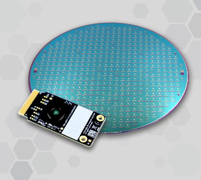
Through innovative engineering, Paragraf has been able to develop a proprietary procedure for synthesising two-dimensional (2D) materials, such as graphene. In contrast to CVD/PECVD, Paragraf’s metalorganic chemical vapour deposition (MOCVD) process, allows graphene to be layered directly onto the semiconductor substrate. The transfer phase that is necessary for other graphene production processes can thus be eliminated, the risk of contamination avoided, and the removal of multiple process steps.
The ability to deposit graphene directly onto wafers (with greater purity and higher degrees of reproducibility) will clearly be advantageous to semiconductor fabs. It will make it possible for the true benefits of graphene to be realised – with certain incumbent materials being replaced by it, in order to heighten performance levels. Thanks to full compatibility with standard semiconductor production procedures, it will be relatively easy for them to integrate the graphene MOCVD into their existing operations.
Graphene in Magnetic Sensing
Hall effect sensors are a non-contact means for measuring the flux density of magnetic fields. These have proved to be an ideal place to showcase Paragraf’s capability to make major upgrades to electronic devices and push performance benchmarks. Standard sensors are limited by the ‘planar Hall effect’, where the in-plane magnetic field can contribute to the output. This limits the resolution or requires more complex measurements and modelling, options that may not be available in real time.
As a 2D material, graphene does not share the directional properties of thicker materials. That is something which is a real differentiator when looking to measure magnetic fields. By using a graphene monolayer sensor element, the errors resulting from erroneous magnetic field components can be removed, allowing superior accuracy to be assured. It is also worth noting that the thermal stability of graphene means that thermal drift which Hall effect sensors normally exhibit can also be minimised. Therefore Graphene-based devices will run at much higher temperatures.
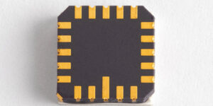
Although, on several occasions, graphene-based Hall effect sensor prototypes have been demonstrated before, none of these would have been able to support full-scale production activities. Paragraf has overcome the obstacles that had previously prevented this and brought the first high volume graphene-based Hall effect sensors to market. The GHS sensors deliver nT resolution levels without the need for additional signal conditioning hardware. Consequently, the sensor system is more streamlined, allowing transparency of the measurement methodology. These devices have a more extensive dynamic range, better linearity and greater temperature stability too. GHS devices are already getting some high-profile endorsements. They have been deployed in the CERN high energy physics research centre, enabling the magnets used in its gigantic particle accelerator to be monitored.
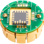 Figure 1: The GHS Hall effect Sensor – First in a Series of Advanced Graphene-Based Devices Developed by Paragraf
The potential of graphene is becoming increasingly apparent to the global electronics business, and MOCVD is allowing its credentials to be highlighted in a commercially viable manner. By synthesising this material in a way that doesn’t require it to be transferred from a metal catalyst, it will be much easier to incorporate into a wide array of different electronic devices.