

It is 10 years since Andre Geim and Konstantin Novoselov, then scientists at the University of Manchester, were awarded the Nobel Prize in Physics for their work on graphene. The extraordinary capabilities of this two-dimensional material, which is made up of a single layer of carbon atoms bonded in a hexagonal array, led to a burst of interest in graphene.
This excitement about graphene led to the creation of a dedicated lab at Manchester to study the material, the launch of a number of start-ups, as well as further academic work on characterising its properties. And yet we are still to see the promise of graphene widely exploited, especially in the electronics industry. Something has been holding it back.
That something is the lack, to date, of a way to make large areas of graphene that can coexist with the manufacturing processes used in the semiconductor industry. Geim and Novoselov famously made their graphene samples by lifting monolayers of carbon atoms from the surface of a block of graphite using sticky tape. Although this served their research needs, it’s not a practical basis for the mass manufacture of large areas of perfect graphene layers.
The key to unlocking the potential of graphene, therefore, is to find a way to make it in large volumes with high consistency and purity. Most graphene commercially produced today is created in one of two ways.
The graphene produced by “exfoliating” graphite (the technique Geim and Novoselov used) is of good quality. The drawback with this approach is that it produces very small areas of graphene, which are also often made up of multiple layers, lack homogeneity, and which cannot be customised. This means it is not really a practical basis for mass-producing electronic devices.
The second approach to making graphene is to deposit it onto a metal substrate, such as copper foil, and then transfer it onto an electronics-compatible substrate, such as silicon. Unfortunately, the various wet and dry processes involved in making the transfer can leave copper atoms behind, affecting how the graphene functions in an electronic device.
This lack of a contamination-free, transfer-free, large-area graphene manufacturing process has limited the material’s adoption in mass-market electronics. A new approach is needed.
Novel technique holds real promise
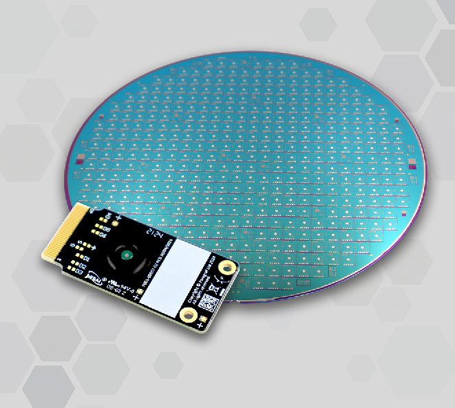
Step forward Paragraf who have developed a way to make large areas of high-quality graphene. The proprietary technology enables the production of high-quality graphene on semiconductor wafers of up to 8in diameter.
The Paragraf chemical vapour deposition technique doesn’t need the transfer processes commonly applied in most large-area graphene synthesis methods. Instead, graphene is produced in a uniform layer directly on semiconductor-compatible substrates such as silicon, silicon carbide, sapphire, or gallium nitride. The resultant graphene monolayer is also free of residual metal atom contaminants present in other techniques that employ a carrier foil.
This approach overcomes many of the obstacles to developing graphene for electronics applications. The next step is to demonstrate this by identifying suitable applications and then bringing commercially viable products to market.
To do this, Paragraf has developed a graphene-based magnetic field sensor that uses the Hall effect, in which a potential difference is formed in a conductor that is subject to a perpendicular magnetic field. Silicon Hall effect sensors already exist, but their sensitivity, accuracy and the range of field strengths they can measure are limited.
The graphene Hall effect sensor offers better measurement performance than silicon devices, for a number of reasons. Graphene is a better sensing medium than silicon because it has a lower “sheet carrier concentration”, that is, there are fewer electrons available to move through the material carrying charge than in competing materials. This gives graphene a sensitivity to magnetic or electrical fields that is 30 to 50 times greater than that of silicon alternatives.
Graphene is also a two-dimensional material, so it lacks the directional properties of bulk materials. In traditional Hall effect sensors, the sensing material’s three dimensionality means that stray magnetic fields, unaligned with the desired sensing direction, are also picked up. This “planar Hall effect” causes measurement errors. Using a monolayer of graphene as a sensor limits the planar Hall effect, enabling more accurate measurement of magnetic fields in the desired direction.
Graphene also has practical advantages as a sensor. It is a strong and robust material, making it suitable for use in industrial environments. It also does not suffer from the same thermal effects as conventional semiconductors. Graphene sensors can work at cryogenic temperatures of less than –271°C (1.8K), which is useful in superconducting environments. They can also be used at up to 150°C (423K). Graphene sensors are also resistant to electrostatic discharge, doing away with the need for protection circuitry.
Graphene Hall effect sensors benefit from very low power dissipation, of the order of picowatts with nanoamperes of drive current, limiting the extent to which they will heat cryogenic environments.
These properties mean that the Paragraf Hall effect sensor offers better performance in a broad range of applications than current devices, according to Dr Simon Thomas, the company’s CEO.
“The sensor’s resolution, combined with the lack of a planar Hall effect, gives it an accuracy that is way beyond what is possible with any other Hall effect sensors on the market. Considering this comes in a small package which is robust in extreme conditions, you end up with a very attractive device that offers comparable performance to fluxgate sensors and NMR probes.”
Field tests provide validation
Field tests with partners have proven the advantages of the Paragraf Hall effect sensor. Paragraf is working with the Magnetic Measurement Laboratory of CERN (the European Organization for Nuclear Research), which has tested the sensors to accurately map the magnetic fields formed within its cryogenic electromagnets. The tests show that Paragraf’s sensor has a negligible planar Hall effect and therefore only takes into account magnetic field components along the desired axis of measurement. CERN is considering using Paragraf’s Hall effect sensors to build a stacked system that will provide a very accurate three-dimensional map of the field within its cryogenic electromagnets.
Paragraf has also been working with the UK’s National Physical Laboratory to investigate the suitability of its sensors for use in extremely harsh environments, and with Queen Mary University of London to study the potential of graphene to replace the indium tin oxide layers often used in touchscreens and displays.
“The Hall effect sensor has already demonstrated its versatility and superiority to conventional sensors in a range of magnetic field measurement applications. The operating temperature range and high sensitivity of the sensor also open up application areas not previously possible,” added Thomas. “For example, the sensors could be embedded into aircraft engines to continuously monitor faults, and once the NPL tests have confirmed that the sensor can operate in harsh radiation environments, it could be used to measure position within nuclear-decommissioning robots and space satellites.”