In this article, Simon Thomas, CEO of Paragraf, outlines ten facts about graphene, its role in the electronics industry, and potential future applications everyone should be aware of.
- Researchers used sticky tape to create the first graphene
When the first graphene available for research was produced back in 2004, it was created using the ‘Scotch tape method’ – an exfoliation process involving the use of sticky tape to pull carbon layers from the top of a graphite block. Since then, several alternative methods have been developed. One option is to grind or pulverise a block of carbon to create graphene nanoparticles. Another way to achieve graphene is liquid phase epitaxy (LPE), which involves evaporating or pulverising liquids that contain carbon to form platelets or films on surfaces. Sublimination, on the other hand, involves thermally reducing carbon-containing solids, so only carbon is left on top of the solid. Finally, some manufacturers opt for chemical vapor deposition (CVD) or plasma-enhanced chemical vapor deposition (PE-CVD), which focus on reacting carbon-containing gases at high temperatures.
- Unrivalled benefits make graphene a wonder material
Graphene is frequently referred to as the wonder material, with good reason. It is over 100 times stronger than steel while being extremely light, over 100 times more conductive than silicon and features the lowest resistivity of all known materials at room temperature. When you combine this with optical transparency of over 97 percent, high flexibility, the highest thermal conductivity of any material, and thermal and chemical stability, the potential is staggering. Graphene is the first single material that can offer all these benefits. These characteristics mean that graphene can help enhance many existing technologies in the electronics sphere as well as across other industries and help overcome challenges that have hindered the development of new technologies.
- Graphene could be the revolution the electronics industry is waiting for
Graphene is ideally suited for electronics applications, thanks to its high thermal and electrically conductive properties, as well as its lightweight nature, being only one atom thick. The electrons in graphene have much higher mobility, and hence speed under an applied electric field, than semiconductors, such as silicon, that are widely used in electronic devices. Therefore, using graphene makes it possible to create more efficient devices that operate faster than conventional alternatives while using less power. Even though graphene is lightweight and flexible, it is significantly stronger mechanically than standard semiconductors, enabling it to tolerate much higher voltages. This is likely to become increasingly vital as all sectors of society look to embrace a greater degree of electrification. Additionally, when operating at these higher powers, graphene’s thermal stability and ability to conduct heat away rapidly reduce device complexity and materials costs. Ultimately, this unique combination of characteristics can help enable entirely new applications in the electronics industry.
- Different types of graphene enable different technologies
There are three main groups of graphene products and technologies. Small particulate, or platelet, graphene is often supplied in a liquid and referred to as graphene suspension. Graphene flakes, typically around 5mm or smaller in size, are usually free-standing and easy to handle with simple tools. Finally, large-area graphene consists of layers of graphene supported on a substrate material, which can be up to 8 inches in size. Each type of graphene can be used for a wide range of applications. For example, simple exfoliated flakes have long been used in research and development to demonstrate in lab-scale applications what graphene can do as an electronic material. They have also been used to make transistors that could potentially lead to electronic products that operate much faster, with lower power consumptions and weigh far less than existing electronics. The material can also lead to much more sensitive sensors, which could be game changing in applications such as medical diagnostics. Even in small particulates, graphene offers exceptional wear resistance and strength, making it highly useful as an additive in materials, solutions, and composites. Graphene paints, for example, have been shown to reduce water friction on ships’ hulls, making operation more efficient. Alternatively, they have also been used to further enhance the high strength properties of carbon composite materials used in aircraft wings. Large scale graphene, on the on the other hand, is crucial for enabling the scaling-up and commercialisation of graphene products, particularly electronics.
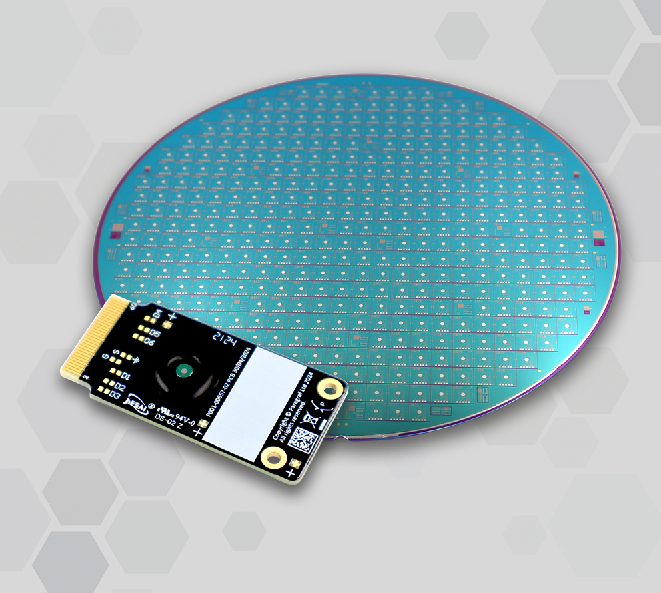
- Paragraf’s proprietary graphene technology is fundamentally different
Paragraf has developed and perfected, a process for depositing single-atom-thick materials, such as graphene, that offers several unique benefits. Chief amongst them is the ease of use: Paragraf’s method results in graphene being produced on top of standard substrates, such as silicon, sapphire, and semiconductors, making it compatible with today’s manufacturing techniques, equipment, and infrastructure. It is also silicon technology compatible, in contrast with many existing graphene forms, which have high levels of contamination arising from the manufacturing technique used. Therefore, graphene can be directly plugged into the electronics device manufacturing chain, enabling it to be used like current standard materials. Crucially, unlike many other manufacturers, Paragraf fabricates graphene using a process called MOCVD (Metalorganic Chemical Vapor Deposition). This is key to overcoming the challenges associated with graphene created by conventional CVD (Chemical Vapor Deposition), such as purity and reproduction issues. Thanks to this innovative approach, for the first time, graphene is now available in forms and formats that will allow the scaling of single device lab prototypes to large scale, volume manufacturing. These technological advances indicate that graphene has real potential to enhance or even directly replace standard materials in many electronic devices, unlocking new levels of end technology performance.
- Graphene brings unprecedented accuracy to magnetic sensing
As graphene’s sheet carrier concentration – the number of electrons per unit area able to move through the material carrying charge – is very low, the material can be up to 50 times more sensitive than a standard semiconductor, such as silicon. This is a significant advantage when configuring the material to interact with other electrical or magnetic fields, for example, in a Hall Sensor. Furthermore, graphene is very robust and doesn’t suffer from the thermal impacts that affect conventional semiconductor devices, which allows the sensor to work in extremely high and low temperatures, including the ultra-low cryogenic range.
- Graphene drastically reduces the Planar Hall Effect
As a two-dimensional material, graphene doesn’t exhibit the same directional properties as thicker or bulk materials, such as silicon. This is particularly important when it comes to Hall Effect sensors, as it helps mitigate an undesired feature called the Planar Hall Effect. Typically, three-dimensional materials are more prone to the Planar Hall Effect where out of plane fields can interfere with the measurements from the desired sensing plane causing spurious results. The single-atom thick structure of graphene (i.e. the lack of a third dimension) helps eliminate these errors and achieve higher precision mapping of magnetic fields. That’s why graphene sensors can offer far superior performance compared to traditional Hall Sensors. They can also be used in applications that traditional technologies have not been able to address, for example in extremes of radiation and temperature.
- Paragraf pioneered the graphene-based Hall Effect sensor
For its first commercial application, Paragraf wanted to create a product that would demonstrate the power of graphene and highlight the advantages it offers when used as an electronic sensor. The company targeted a ubiquitous sensor to demonstrate the performance enhancement graphene can bring to a well-known electronic device and hence present a test case for graphene’s real-life potential. Paragraf’s hypothesis was that the performance of these legacy devices could be significantly improved with sophisticated graphene technologies. The resulting performance improvements could benefit many applications where accuracy is vital, including medical diagnostics, vehicle drive train efficiency, and global positioning.
- Paragraf’s graphene technology is being tested by CERN
CERN (the European Organization for Nuclear Research) uses high precision and reliable measurement performance for many ongoing projects. That’s why the Magnetic Measurement section of the organisation is continuously looking for new ways to optimise the accuracy of its measurement technologies. Paragraf’s Hall Effect sensor was of particular interest to CERN scientists as, unlike other Hall Effect sensors, it displays negligible Planar Hall Effect, minimising inaccuracies in measurement and delivering much-improved measurement accuracy. This mutual interest in the development of magnetic sensing has led Paragraf and CERN to embark on a partnership to test the Hall Sensor’s capabilities and demonstrate the unique properties graphene opens for magnetic measurements.
- The future spells more cost-effective manufacturing and improved performance
Future applications for graphene are very wide ranging. One of the most exciting areas of application is large-area graphene, which is the key to turning R&D projects into real-world products. With the availability of large-area graphene layers, many different fields of technology are set to benefit, including computing, energy generation, and energy storage. For example, in solar power applications, constraints arising from traditional construction methods currently mean that the solar cells have maximised efficiency at approximately 23-24 percent. However, by supplementing the silicon-based cells with graphene, this performance could be increased by up to three percent – a very significant increase. Paragraf is also currently looking at many other areas where graphene can prove transformative, including as a replacement for indium tin oxide (ITO). ITO is presently widely used in many fields of optoelectronics, as a transparent electrically conductive electrode. It is vital for many applications, but the associated cost and scarce availability of indium present challenges to manufacturers. Here, graphene could prove a good alternative. Its unique qualities could enable it to replace ITO in applications including solar panels, mobile phones, television screens, computers, and organic LEDs.